Our design approaches can be summarized in three classes, Full-custom, All-programmable, Full-custom with Integrated Circuits.
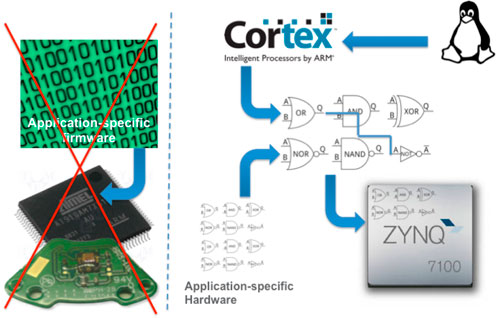
Our design approaches include a standard and consolidated approach based on microprogrammed commercial components, a standard and consolidated all-programmable FPGA design approach aimed at the implementation of fully reconfigurable processing units with custom hardware acceleration and Linux operating system on the same chip (hardware acceleration, software drivers and operating system tweaked and patched in-house) and, a more research-oriented approach aimed at Integrated Circuit (IC) design with particular emphasis on ultra-low power wireless systems.
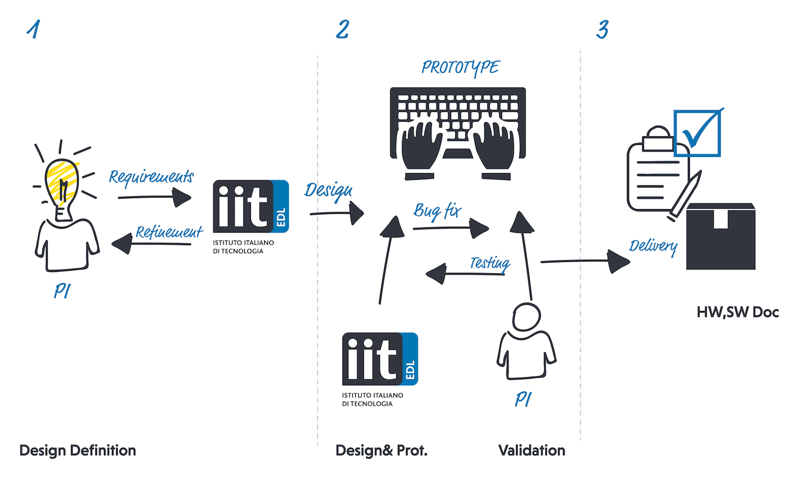
The design flow is typically organized in three phases: i) constraint and requirements definition, ii) development and validation, iii) delivery and technical support.